dstroy
Insanely Active Member
Not all of the power supplies are redundant. Just +24,12,5,3v3 bus voltages. Then +9 and +5v for the microcontrollers.
Two batteries, one main battery and an emergency lipo to charge supercaps. I'll build a chargepump to charge the caps from the battery.
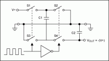
Something like this but with a bank instead of two caps, and +12vout.
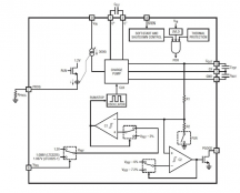
I will have a better idea of what size and discharge rate of battery that I need when I determine the charging characteristics of the supercapacitors and output of the charge pump circuit.
Two batteries, one main battery and an emergency lipo to charge supercaps. I'll build a chargepump to charge the caps from the battery.
Something like this but with a bank instead of two caps, and +12vout.
I will have a better idea of what size and discharge rate of battery that I need when I determine the charging characteristics of the supercapacitors and output of the charge pump circuit.